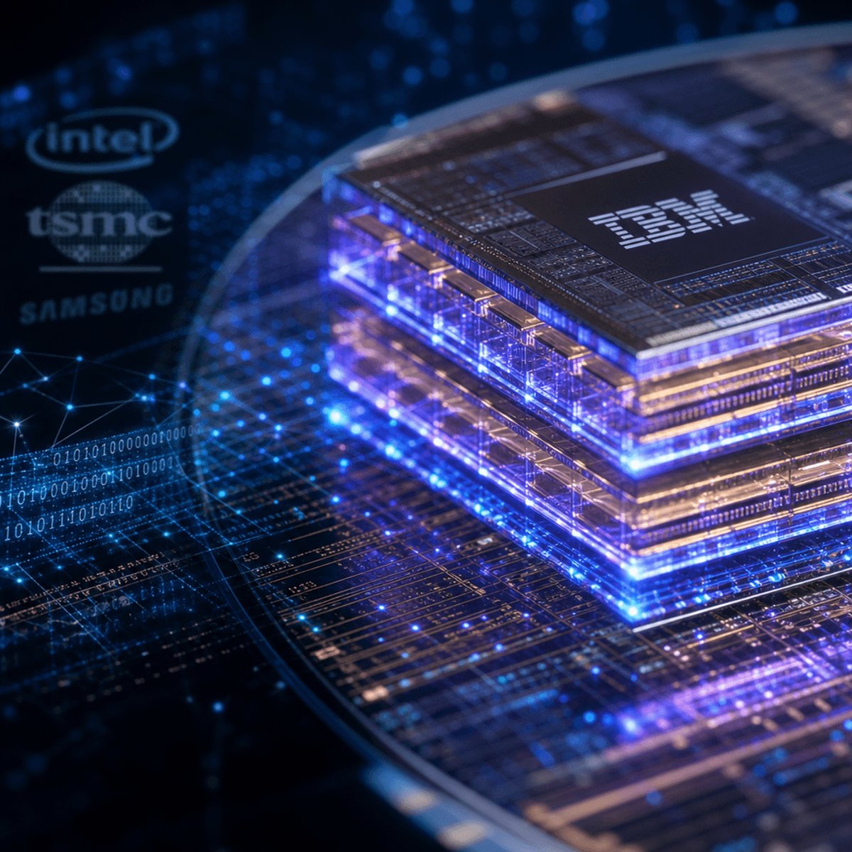
IBM just claimed victory in one of semiconductor manufacturing's most intense competitions. The company announced it's achieved the first sub-one-nanometer chip architecture, cramming nearly 100 billion transistors onto a single die using what it calls "nanostack" technology. The breakthrough shatters previous density limits and positions IBM ahead of rivals like Intel, TSMC, and Samsung in the race to build chips powerful enough for next-generation AI workloads.
IBM dropped a bombshell in the semiconductor world today, claiming it's crossed the sub-one-nanometer threshold with a chip architecture that packs nearly 100 billion transistors onto a single die. The announcement represents a massive leap in a space where progress is typically measured in incremental gains, and it puts IBM squarely ahead of the pack in the chipmaking arms race.
The technology, which IBM calls "nanostack," represents a fundamental rethinking of how transistors are arranged and connected at the atomic level. While competitors like TSMC and Samsung are still ramping production of 3nm chips and planning 2nm nodes for next year, IBM's claiming to have blown past those milestones entirely. The sub-1nm designation isn't just marketing spin - it reflects actual gate lengths that push closer to the physical limits of silicon-based semiconductors.
What makes this particularly significant is timing. The AI boom has created insatiable demand for computing power, and data centers are struggling to keep up. Nvidia's GPU shortages have been well-documented, while hyperscalers like Amazon and Microsoft are racing to build custom silicon. IBM's breakthrough could reshape that landscape by offering dramatically higher transistor density, which translates directly to more computational capability per square millimeter.
The nanostack approach reportedly uses vertical transistor architectures stacked in layers, maximizing three-dimensional space in ways traditional planar designs can't match. This isn't IBM's first rodeo with advanced chip research - the company has a long history of semiconductor innovation, from pioneering copper interconnects to developing silicon-on-insulator technology. But this represents their most aggressive push yet into territory that many thought was still years away.
The 100 billion transistor figure is staggering when you put it in context. Apple's M3 chips, built on TSMC's 3nm process, contain roughly 25 billion transistors. Nvidia's latest H100 GPUs pack around 80 billion. IBM's claiming to fit more transistors into a comparable space, which could mean unprecedented performance for AI training, complex simulations, and enterprise workloads that require massive parallel processing.
Of course, there's a gap between lab demonstrations and mass production. IBM hasn't announced when - or if - these chips will reach commercial manufacturing. The company shuttered its own chip fabrication plants years ago, partnering instead with Samsung and others for production. Translating research breakthroughs into high-volume manufacturing is notoriously difficult, especially at these extreme scales where even minor defects can tank yields.
The implications extend beyond pure performance metrics. As transistors shrink, power efficiency typically improves, which is critical for data centers already consuming massive amounts of electricity. Every generation of density improvement means more computation per watt, directly impacting operational costs and environmental footprint. For cloud providers and enterprises running AI workloads 24/7, that efficiency gain compounds rapidly.
IBM's announcement also raises questions about Intel's ambitious roadmap. The chipmaker has been promising a return to process leadership with its Intel 4, Intel 3, and future angstrom-era nodes. If IBM's sub-1nm claims hold up, it suggests the path forward may require more radical architectural innovations than simply shrinking existing designs. Intel's been investing heavily in gate-all-around transistors and backside power delivery, but nanostack-style approaches could represent the next evolution.
The semiconductor industry has been predicting the end of Moore's Law for decades, yet engineers keep finding ways to squeeze more transistors onto silicon. IBM's breakthrough suggests we're not quite at the physical limits yet, though we're clearly approaching them. Beyond 1nm, quantum effects and atomic-scale variability become increasingly difficult to manage. Some researchers believe entirely new materials - like graphene or carbon nanotubes - may be necessary for the next leap.
For now, IBM's staked its claim as first across the sub-nanometer finish line. Whether that translates to commercial products remains to be seen, but the technical achievement alone signals that the chip wars are far from over. With AI driving unprecedented demand and geopolitical tensions reshaping semiconductor supply chains, breakthroughs like this carry implications that extend well beyond the lab.
IBM's sub-1nm breakthrough isn't just a technical milestone - it's a signal that the semiconductor industry still has room to push boundaries despite decades of predictions about hitting physical limits. The real test comes next: can this lab achievement translate to commercial manufacturing at scale? If IBM and its fabrication partners crack that challenge, we're looking at a fundamental shift in what's possible for AI infrastructure, enterprise computing, and data center efficiency. For now, the company's seized the narrative in the chip race, and competitors will be scrambling to respond. The question isn't whether sub-nanometer chips are possible anymore - IBM just proved they are. The question is who can bring them to market first, and what comes after we've exhausted silicon's final tricks.